


The SW and LW gratings are associated with 4 different detector arrays
of 12 elements each, and the 2 SWS Fabry-Pérots are associated with 2
double detectors (only one of each pair being used to gather valid
data). More information on the detectors is given in Table
2.1. All
![]() detectors
are operated simultaneously. The InSb, the Si:As (BIBIB) and the Si:Ga
detectors are operated at a temperature of 4 K, which is the
temperature of the spectrometer unit. The Si:Sb detectors for the FP
are heated to 10 K and the Ge:Be detectors are cooled to 2.5 K by a
thermal strap to the helium tank of the cryostat.
detectors
are operated simultaneously. The InSb, the Si:As (BIBIB) and the Si:Ga
detectors are operated at a temperature of 4 K, which is the
temperature of the spectrometer unit. The Si:Sb detectors for the FP
are heated to 10 K and the Ge:Be detectors are cooled to 2.5 K by a
thermal strap to the helium tank of the cryostat.
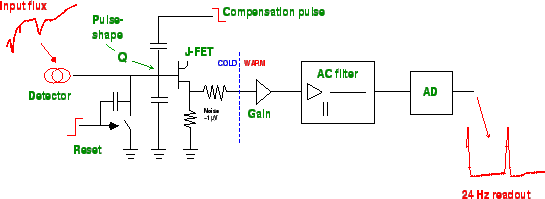
Except for the InSb photo-diodes, the detectors are photo-conductors that require a finite bias voltage. The detectors are connected to discrete integrating-amplifier chains. The first amplifier stages are heated-JFET buffer amplifiers located close to the detectors. The remaining electronics are located in the warm amplifier box in the service module of the satellite.
|
A schematic diagram of the detector electronics is shown in Figure 2.6. The detector current charges the small capacitor formed by the finite capacitance of the JFET gate and of the electrical leads between the detector and the gate. The resulting voltage ramp is amplified and digitised, to be read out `non-destructively'. Every 1, 2 or 4 seconds (selected by the AOT logic) the pre-amplifier is reset by removing the charge from the input gate. The residual charge after a a reset is minimised by a compensation pulse immediately following the reset.
The heated-JFET pre-amplifiers of each grating detector array are combined in a single integrated circuit. A side-effect of this arrangement is that stray capacitance between the input leads of the pre-amplifiers causes significant cross-talk between neighbouring array elements. Since the only involved impedances are capacitive, the cross-talk percentage is independent of frequency and can be accounted for in the data analysis.
The pre-amplifier resets are sufficiently compensated to avoid overloading of the first stages of the warm amplifiers. To avoid dynamic-range problems due to remaining offsets, the signals pass through an AC filter that removes the DC offset. This filter affects the shape of the ramps in a predictable and correctable fashion.
The filter outputs are sampled 24 times per second, and then they are multiplexed. They pass through an amplifier with selectable gain factor of (1, 4 or 16) times 225. The gain for FP detectors is an overall factor of 2 higher. Finally they are digitised into 12-bit numbers (covering a 20-V range). At the highest gain setting, the digitisation is precise enough to sample the pre-amplifier noise. At the lowest gain setting, the gain of the warm amplifiers is 225 for the grating detectors and 450 for the FP detectors.
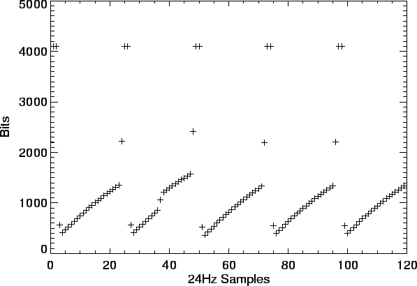
Figure 2.7 gives a data example in which the individual datapoints from the non-destructive readouts and reset pulses can be seen. The plot starts with a reset pulse, where the capacitor is short-circuited causing the bit readout to spike high. The system stabilises after about four readouts, and as light falls on the detector the charge on the integrating capacitor slowly increases. Careful analysis shows the system to require more than four readouts to stabilise. All the slopes are slightly curved, due to the limited time constant of the AC filter - see Chapter 7. The second slope suffers from a glitch approximately half way along its length, where the measured voltage suddenly jumps instead of following the (curved) slope. Some extra charge is dumped on the capacitor due to e.g. a cosmic ray hit. The rest of this readout is not affected by the glitch as the slope just continues on its curved path, as can be seen by comparing it with the other four slopes.
Data examples for each AOT are shown in Sections 3.3 to 3.6. The automatic data processing chain (OLP) is discussed in Chapter 7.
|
In this section all processes that can be identified in the 24 Hz data or in the extracted spectrum induced by the detectors and electronics will be briefly described. This is adapted from Lahuis et al. 2001, [25].
Transient effects were observed in the laboratory prior to launch and have been taken into account in the design of the observing templates used for all general observations. The templates were designed such that the influence of transient effects were minimised. There is sufficient redundancy in each observation so that transient effects can be recognised in the time domain and possibly corrected for. Memory effects are discussed further in Sections 7.3.3.2 and 9.2.
Unless otherwise noted, these effects are corrected for in the pipeline in the reverse order in which they occur, to undo their effects and to reconstruct the incoming signal. See Section 7.2.