


The CRE output voltage of the first few readouts on a ramp does not follow a linear increase in time but can remain constant or even show a decrease in voltage. The effect becomes more pronounced in case only a small fraction of the CRE dynamic range is used. This can happen in observations where the source + background flux was severely overestimated by the observer or in the low brightness regions of maps with high dynamic range.
To exclude this non-linear part of a ramp, the first fraction of the total number of non-destructive readouts is discarded in the SPD processing. The value of the fraction is stored in a dedicated calibration file (see Section 14.4)
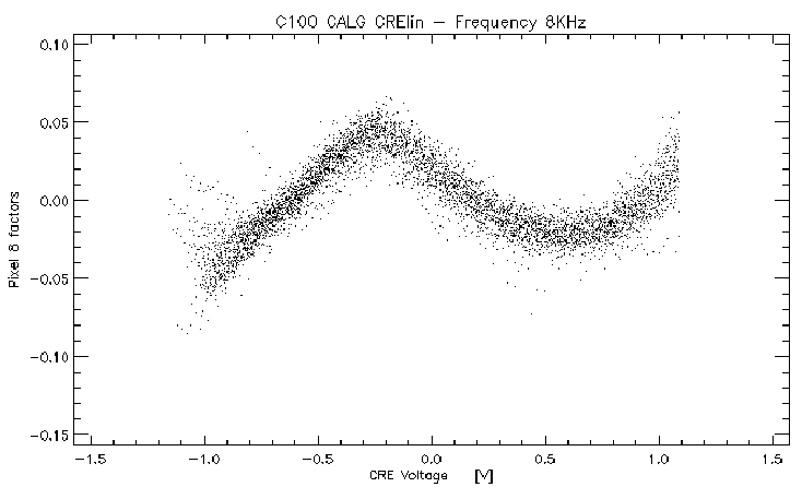
Integration ramps are not exactly linear but exhibit higher order variations or in some cases `knees' which are caused by the CRE. The deviations from linearity only depend on the absolute value of the CRE output voltage and not on e.g. the slope of the ramp (see Schulz 1993, [50]). Non-linearities can cause systematic errors up to 50% when comparing signals from the same source using ramps with different dynamic range in CRE voltage. This effect introduces an error in the flux calibration in case the FCS readouts span a different dynamic range than the source readouts. Improper correction for ramp non-linearities can also cause serious systematic brightness errors in maps with high dynamic range between background level and target. In addition, ramp non-linearities introduce a larger formal uncertainty in the signal when deriving a signal value by fitting a straight line through the ramps.
The deviations from linearity for all detectors except for PHT-SS and SL have been determined with respect to a standard linear ramp which was constructed from a stack of several thousand individual ramps. An example of the resulting deviations is presented in Figure 4.5.
|
In the SPD processing the CRE output voltage for each readout is corrected before deriving the signals. Calibration tables for the P, C100, and C200 detectors have been created containing CRE output voltages and the corresponding voltage corrections. These calibration tables are stored in Cal-G files (see Section 14.5).
Non-linearities in the CRE output of PHT-SS/SL data are not corrected for. Due to the selected calibration scheme for this detector where a standard source is chosen as close as possible to the output signal, the uncertainty imposed by this effect should be negligible.
Measurements of a given target obtained with the same detector/filter/aperture combination but with different readout timing (ROT) parameters showed that the signal depends on the commanded reset interval (see Section 2.4.4). For a constant detector illumination the signal level varies systematically from one reset interval to the other. The systematic variations are probably caused by the detector CRE (Section 2.4.2) while switching between different reset interval times.
For C100 and C200 these variations are of the order of 10-20% between measurements which differ in reset interval by a factor of 2. For reset intervals a factor of 8 apart the signal difference can be as large as 40%. P1, P2 and P3 show less variations. For the detectors of PHT-S the situation has not been investigated.
As long as the FCS calibration measurement is obtained with the same reset interval as the target measurement no error is introduced and therefore no corrections are necessary. But for the majority of the PHT observations with PHT-P and PHT-C, different measurements of the same AOT using the same detector were obtained with different reset intervals.
An empirical correction has been derived based on calibration observations where the same flux was observed with different reset interval parameters. It is found that signals measured with 2 different reset intervals show a linear dependence:
where, ![]() and
and ![]() (in V/s) are the signals obtained with reset
intervals
(in V/s) are the signals obtained with reset
intervals ![]() and
and ![]() and
and ![]() (in V/s) is the offset and
the dimensionless
(in V/s) is the offset and
the dimensionless ![]() is the slope of the regression.
is the slope of the regression.
Once the relative signal variations between different reset intervals of the same detector are known, a signal (in V/s) can be corrected with respect to a reference reset interval according to the following relation:
| (4.6) |
where the reference reset interval was chosen to be
![]() ,
and the constants
,
and the constants ![]() and
and ![]() refer to the reference reset interval
refer to the reference reset interval
![]() s. The correction assumes a data reduction of 1 (see
Section 2.4.4) for the corrected signal. The correction
parameters together with their uncertainties are stored in
Cal-G files - see Section 14.6
s. The correction assumes a data reduction of 1 (see
Section 2.4.4) for the corrected signal. The correction
parameters together with their uncertainties are stored in
Cal-G files - see Section 14.6
The transformation of all signals to an equivalent signal obtained with
the reference reset interval has the consequence that the standard dark
signals must also be transformed. Due to this correction, the dark signals
for ![]() s of a given detector can have a negative value (see
Section 14.7.1 for a description of the calibration
file). This has no physical meaning, but reflects the zero point in the
ISOPHOT signal calibration.
s of a given detector can have a negative value (see
Section 14.7.1 for a description of the calibration
file). This has no physical meaning, but reflects the zero point in the
ISOPHOT signal calibration.
The accuracy of the correction is strongly coupled to uncertainties in the ramp linearisation correction (Section 4.3.2). In addition, the uncertainty increases for readout settings far outside nominal working range of the integration ramps. The calibration observations for the reset interval corrections have been optimised for signals with ramps in the range of 20% to 200% of the maximum unsaturated CRE voltage. For signals outside this range, the uncertainties in the corrections can be as high as 20-30%. It was found for the C100 detector that the consistency of the correction among the detector pixels quickly drops for ramps that are close or higher than the ramp saturation limits due to improper ramp non-linearity corrections.
The C200 detector exhibits a breakdown of Equation 4.5 for measurement times longer than 1800 s due to instabilities in the CRE performance. If these instabilities occur, they affect usually long mapping observations with C200 where the flux level during the measurement is nearly constant.
For the P1 detector, the reset interval correction was found to depend on the operating temperature of the detector and CRE. During operations after revolution 78 the P1 operating temperature was nearly constant at 2.9K, but before that revolution (during Performance Verification phase) the operating temperature was 2.4K. It is therefore recommended to be cautious applying the reset interval correction to P1 observations collected before revolution 78; the temperature as well as the reset interval difference between the FCS and sky measurement should be verified first.
Detectors PHT-SS, PHT-SL, and
PHT-P1 are high bias, PHT-P2
medium and the PHT-P3, -C100,
-C200
low bias detectors (see Table 4.3).
For the low bias detectors de-biasing occurs when the full
integrator voltage range is used. Infrared photons induce charged carriers
in the detector which are accumulated on the feedback capacitor of the
readout electronics (![]() , see Figure 2.5) during the
integration. An electrical field is built up which reduces the actual bias.
The stronger the illumination, the stronger the field and herewith the bias
reduction4.1. For
the C200 detector the effect is strongest: the bias can drop by a factor
of about 2 from 80 down to 40 mV. This effect causes the ramps to become
non-linear with a downward curvature (Wolf, Grözinger & Lemke
1995, [58]).
, see Figure 2.5) during the
integration. An electrical field is built up which reduces the actual bias.
The stronger the illumination, the stronger the field and herewith the bias
reduction4.1. For
the C200 detector the effect is strongest: the bias can drop by a factor
of about 2 from 80 down to 40 mV. This effect causes the ramps to become
non-linear with a downward curvature (Wolf, Grözinger & Lemke
1995, [58]).
In contrast to the CRE ramp non-linearity (Section 4.3.2), the non-linearities caused by de-biasing depend on i) the CRE reset level (see Section 2.4) which can float and ii) the strength of the photo-current. This complicates possible solutions for correction. Presently no distinction is made between de-biasing and CRE non-linearity when correcting the ramps. For a given detector, there is one correction table taking care of both effects. Section 7.2.8 describes the correction that has been applied by the SPD processing software.
Consequently, signals are more underestimated the stronger the signals are. Signals derived from partially saturated ramps (Section 4.3.5) suffer most noticeably from this effect. Observers who collected maps with high dynamic range in bright regions using P3, C100, or especially C200 should be aware of this effect before interpreting their results.
In addition, for high signals on low bias detectors charges on the feed-back capacitor can cause an increased glitch rate (Section 4.4) of the detector.
If the astronomical source is brighter than anticipated, it may happen that parts of the integration ramps are saturated, i.e. the maximum CRE voltage level is reached before the next destructive readout. For most detectors the subsequent readouts after saturation remain at the maximum CRE voltage level until the next destructive readout. However, for some detectors the voltage of the saturated readouts can drop back below the threshold voltage.
The same can occur in case the actual detector responsivity exceeds the nominal responsivity by a large factor. A nominal responsivity was used to a-priori set the ROT parameters before execution of the observations.
The readouts taken during CRE saturation cannot be used and should be discarded. During SPD processing, all readouts in a ramp that are subsequent to a saturated readout are removed (Section 7.2.7). The threshold CRE voltages for saturation are presented in Table 4.4.
| Detector | Threshold [V] |
| P1 | 1.091 |
| P2 | 1.091 |
| P3 | 1.097 |
| C100(1,2,3) | 1.063, 1.088, 1.095 |
| C100(4,5,6) | 1.097, 1.098, 1.099 |
| C100(7,8,9) | 1.098, 1.098, 1.097 |
| C200(1,2) | 1.091, 1.090 |
| C200(3,4) | 1.091, 1.088 |
| PHT-SS(1..64) | 1.040, 1.093, 62 |
| PHT-SL(1..64) | 1.007, 1.099, 62 |
The signal per ramp can still be determined from the reduced number of readouts that remain below the CRE threshold voltage.
The destructive readouts are synchronized with the chopper transitions. The synchronisation pulse triggering the chopper transition disturbed the subsequent integration. As a consequence, the first ramp of each chopper plateau stacks clearly out of the sequence of ramps. In case of a staring measurement, a chopper transition with zero deflection (a so-called virtual chopper transition) occured each 128 s.
For the disturbed ramps the CRE reset level (see Section 2.4.2) is high and also the ramp signal can be different from the average signal derived from the other ramps of the corresponding chopper plateau.
For staring mode observations, for which the signals are derived per ramp, the SPD processing discards the first ramp per chopper plateau and does not take it into account when computing the average signal. For chopped mode observations, for which signals are derived from read-out pairs in order to have a better statistics due to the limited number of ramps per chopper plateau, also the data from the first ramp of each chopper plateau are considered in the biweight mean computation. In case this ramp produces significant signal outliers they are discarded in the biweight mean computational process.
The CREs for the ISOPHOT detectors were fabricated in CMOS technology. A known phenomenon of CMOS devices is the occurence of high supply currents after switch-on, which is called latch-up. The effect is due to the presence of a parasitic transistor in the CRE. A small amount of charge left in the basis region of this transistor can cause it to conduct thereby creating the high supply current. Latch-ups could be recognised by an increased voltage on one of the CRE supply lines. This supply voltage was monitored by the instrument controllers.
During the instrument activation sequence at the beginning of each revolution a latch-up recovery was performed which reset the CREs into their nominal status. The recovery procedure consisted of pseudo measurements of 1 s length which selected and subsequently deselected the individual CREs.
Besides the switch-on effect some CREs tended to show latch-up effects during the science window. Two types of latch-ups could be distinguished: 1) A spontaneous latch-up which was associated with the C100 and C200 devices towards the end of the mission. This latch-up was not correlated with any selection of the device but was cured whenever the device was selected for a measurement and thus was harmless. 2) An induced latch-up which was associated with the P2 device after selecting it when powering up the heater. This latch-up persisted during the measurement and caused noisy integration ramps.
In the beginning of the mission only P2 latch-ups happened. When a latch-up event occured, the measurement was aborted in real time by the instrument controllers. Subsequently they had to initiate a latch-up recovery procedure. Due to the duration of this procedure also the following AOT could be skipped. All affected AOTs were flagged as failed and the observations entered the queue for rescheduling.
As a first counter measure to prevent P2 latch-ups, the latch-up recovery sequence was included in the switch-on sequence of the P2 detector. This way of operation did not work properly either. The final fix was to select the P2 CRE only after a sufficient stabilisation time of the P2 heating which caused some additional overhead in the AOT execution time. P2 was operated in the original latch-up susceptible mode up to revolution 270. From revolution 270 to revolution 690, the mode with the pseudo measurements was applied. Afterwards P2 was operated in the final and stable mode. It should be noted that AOT PHT03 which combined measurements of P1 and P2 never failed (those had by design the switch-on of the P2 heater and the long stabilisation time from the beginning).
The pseudo measurement is present in the telemetry data (of revolutions 270-690) but is removed in Derive_ERD and should be transparent to the observer who starts processing from ERD.
The spontaneous latch-ups of C100 and C200 devices were at the end of the mission practically permanently present, as long as the device was not selected for measurement. As mentioned above, there was, however never any impact on any measurement.